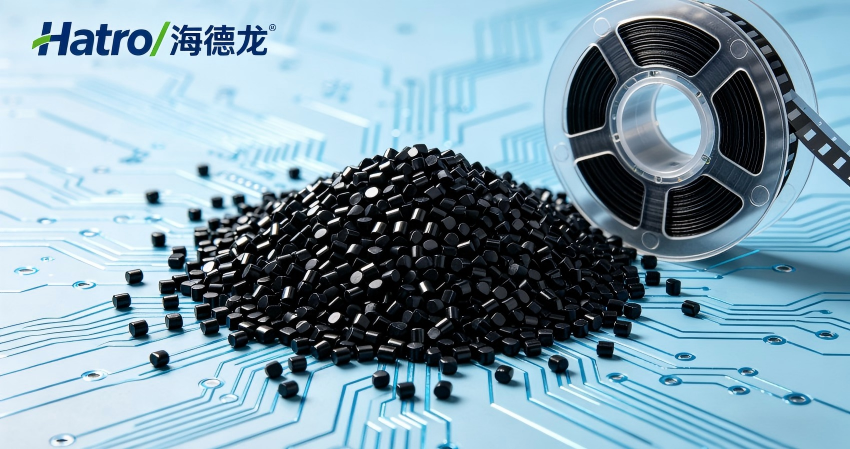
Behind carrier tapes, reels, trays and other critical semiconductor packaging components, conductive PS raw material is the key to ESD protection, dimensional stability and molding performance.
For more than 20 years, this core material has been tightly monopolized by overseas manufacturers: closed formulas, high prices, unstable lead times and strict technical blockades have left the domestic semiconductor packaging industry in a long-term “bottleneck” situation.
With years of deep cultivation in semiconductor packaging materials, Hatro insists on full-chain independent research and development and officially launched EC-55 conductive PS raw material. With stable performance, mature mass production and controllable costs, it has become a benchmark material for domestic substitution, freeing small and medium-sized packaging components from import dependence.
The 20-Year Bottleneck: Why Conductive PS Matters
Conductive PS is not ordinary plastic—it is the first line of ESD defense in semiconductor packaging.
- Stable surface resistivity is essential to avoid electrostatic breakdown of sensitive components
- Molding and toughness directly affect the yield of carrier tapes and reels
- Cleanliness, low precipitation and environmental compliance are mandatory for high-end packaging
In the past, domestic enterprises could only purchase imported materials at high prices, facing high costs, weak bargaining power and constant risks of supply cuts, leaving the entire industrial chain vulnerable.
EC-55: Benchmark Domestic Basic Grade, Stable & Cost-Effective
Hatro EC-55 is our first self-developed conductive PS designed for general semiconductor packaging scenarios, ideal for small and medium-sized carrier tapes, standard reels and conventional trays.
1. Stable & Controllable Conductivity
- Surface resistivity: 10⁶–10⁹ Ω/sq
- Uniform static dissipation without accumulation or rebound
- Fully meets anti-static requirements for SMT placement, storage and transportation
2. Excellent Molding & Dimensional Stability
- High-purity PS substrate with uniform melt flow for precision extrusion and injection
- Balanced toughness, resistant to cracking and whitening
- Strong dimensional stability during winding, insertion and stacking
3. Low Precipitation & High Cleanliness
- Low volatility and low mold contamination
- RoHS & REACH compliant, suitable for clean production rooms
- No harmful substances or unpleasant odors
4. Independent R&D with Lower Cost
EC-55 is developed with full independent intellectual property rights, including formula system, filler dispersion and processing technology:
- Significantly lower cost than equivalent imported materials
- Stable supply unaffected by global logistics and policies
- Faster delivery and more responsive local service
Application Scenarios
- 8mm / 12mm standard carrier tapes
- 7×8, 7×12 semiconductor reels
- General ESD trays and boxes for SMT lines
- Packaging for 0402/0603, SOT23 and other small components
- General packaging requiring balanced ESD, mechanical properties and cost control
The First Step of Domestic Replacement: From “Usable” to “Reliable”
EC-55 represents more than a single material—it is the first breakthrough of domestic conductive PS against foreign blockade.
It proves that Chinese enterprises can independently research, produce and control the supply chain, no longer at the mercy of overseas suppliers.
Choose EC-55 for:
✅ Freedom from foreign technology bottlenecks
✅ Controllable costs and healthier margins
✅ Stable supply and safer production lines
✅ International-level quality supporting domestic semiconductor growth